We offer our customers one or a combination of checks and tests from the following offer.
What are the basic procedures behind DPS testing?
PCB inspection

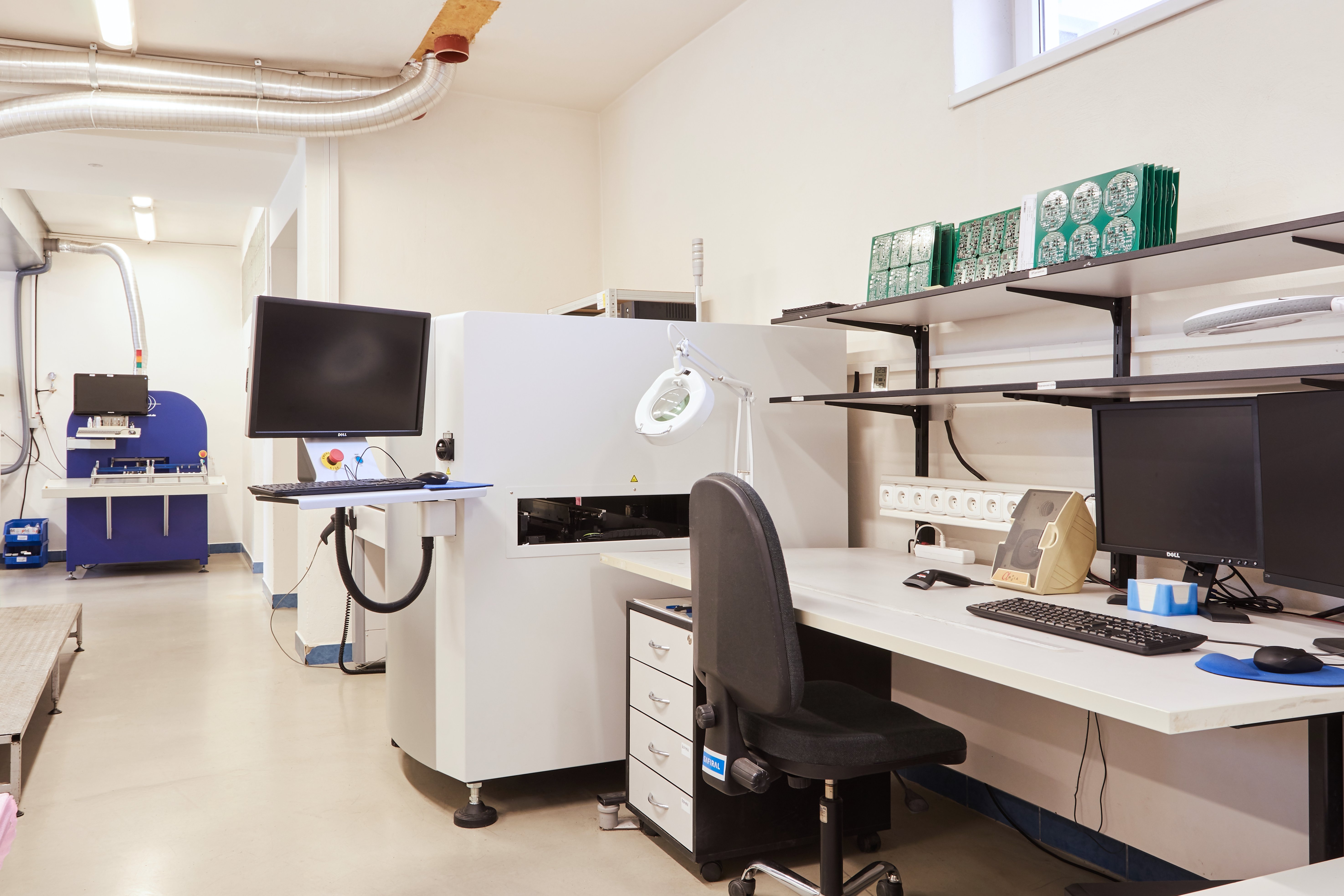
Fully automated inspection with the SAKI 3Di-LS2-A 3D AOI (Automated Optical Inspection) device
AOI uses a combination of 2D and 3D inspection technologies to detect various types of defects, including:
- missing components
- their incorrect location
- raised conductors
- defects of soldered joints
- AOI has multiple cameras and laser sensors to capture images of the PCB from different angles, enabling the detection of defects that may not be visible with traditional 2D inspection methods. The program compares photos of your board with a detailed diagram.
- AOI can be useful for early detection of problems to ensure that production is stopped as quickly as possible. However, it does not revive the board and may not have 100% coverage for all component types.
- The AOI 3Di-LS2-A include high-speed inspection - up to 100 cm² of PCBs per second can be inspected. Other device functions include checking the height and shape of the components placed on the PCB. In addition, the AOI 3Di-LS2-A uses advanced algorithms to analyze inspection data and minimize the number of false alarms, reducing the need for manual inspection and subsequent rework.
- In practice, we should rely on more than automated optical inspection but combine it with another test. A frequently used combination is AOI and ICT or AOI and functional testing.
Optical inspection of mounted printed circuit boards is included in the comprehensive price offer you will receive from us. It is an automatic and nowadays standard part of our production process.
X-ray inspection with X-ray system Sciencecope X-Scope 3000
X-ray inspection (also AXI) makes it possible to detect defects that may not be visible with other test methods. The Sciencecope X-Scope 3000 X-ray inspection system uses a combination of X-ray technology and advanced image processing software to provide detailed images of the internal structure of electronic devices.
The X-Scope 3000 can produce high-resolution images down to 1 micron, enabling the detection of microscopic defects. Soldered joints or usually hidden elements, such as BGAs with joints under the case, are inspected. The X-ray detects possible short circuits before connecting the voltage and thus preventing damage to the component or the entire assembly. The device supports multiple inspection modes, including transfer mode (remote view), oblique mode (at an angle), and laminography mode. Inspection of TH and SMD components for surface mounting is a matter of course.
Overall, the Sciencecope X-Scope 3000 X-ray inspection system is a powerful tool for detecting defects in electronic equipment and ensuring its quality and reliability. Although this inspection can be beneficial, it requires trained and experienced operators. It is essential to check each layer of the board. It is a time-consuming process.
If you want to use the X-ray inspection service for your products, please include this information in the inquiry addressed to the sales department. The service is charged at 160 EUR/hour. In the case of a request to check the PCB in the order of pieces, the price is set at 8 EUR/frame.
Testing and checking directly in the production line
Funkcional Testing
The functional testing service will be especially appreciated by customers during the implementation of a complete order, the so-called "out of box" when the final product from us goes directly to distribution. Functional testing is required to switch on (revive) the electronic device to work without problems.


